

This demo illustrates the use of the SAR ADC and BCTU modules, where ADC conversions are initiated through a BCTU software trigger. The implementation relies on RTD high-level (MCAL) drivers to perform ADC channel conversions.
The BCTU operates in Control Mode, taking full control of the ADC module and managing all ADC sampling through software-triggered conversions. Instead of sampling external analog inputs, the ADC channels are configured to measure the internal bandgap reference and VREFH voltage, typically around 1.2 V and 5 V, respectively.

This example was developed using the FRDM Automotive Bundle for S32K3 + S32M27. To download and install the complete software and tools ecosystem, use the following link:
- Type-C USB cable
- Personal Computer
- FRDM-A-S32K344
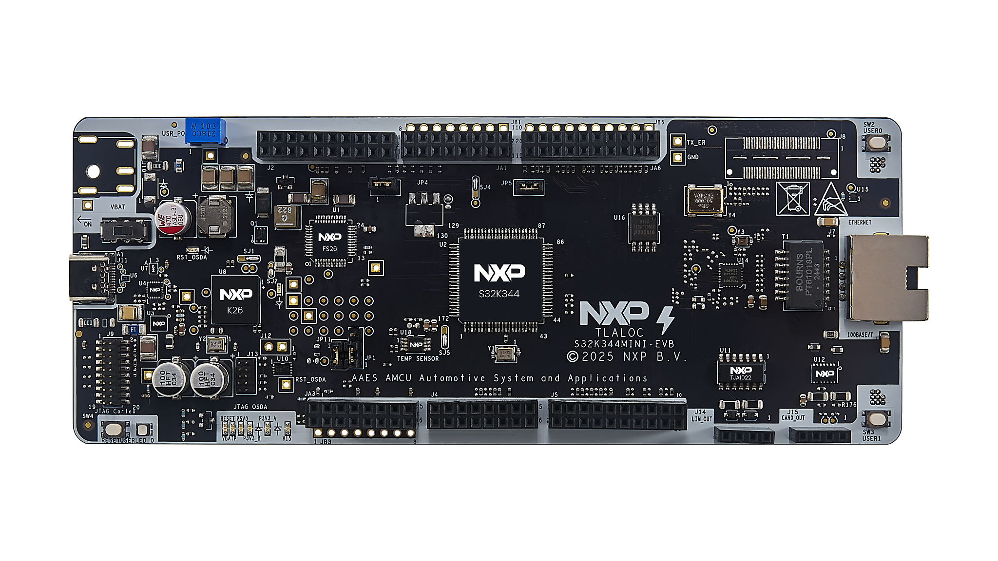
-
Open S32 Design Studio IDE, in the Dashboard Panel, choose Import project from Application Code Hub.

-
You can find the demo you need by searching for the name directly "BCTU Control of ADC Sampling". Open the project, click the GitHub link from this window, S32 Design Studio IDE will automatically retrieve project attributes then click Next>.

-
Select main branch and then click Next>.
-
Select your local path for the repo in Destination->Directory window. The S32 Design Studio IDE will clone the repo into this path, click Next>.
-
Select Import existing Eclipse projects then click Next>.
-
Select the project in this repo (only one project in this repo) then click Finish.


-
In Project Explorer, right-click the project and select Update Code and Build Project. This will generate the configuration (Pins, Clocks, Peripherals), update the source code and build the project using the active configuration (e.g. Debug_FLASH). Make sure the build completes successfully and the *.elf file is generated without errors.
Press Yes in the SDK Component Management pop-up window to continue.
-
Go to Debug and select Debug Configurations. There will be a debug configuration for this project:

 Configuration Name                  Description
 -------------------------------     -----------------------
 $(example)_debug_flash_pemicro      Debug the FLASH configuration using PEmicro probe
Select the desired debug configuration and click on Debug. Now the perspective will change to the Debug Perspective. Use the controls to control the program flow.


The demo is divided into 3 parts:
Part 1: BCTU control mode, using list mode for conversion on all ADC instances in series, data conversion is updated by DMA.
Part 2: BCTU control mode for parallel conversions from all ADC instances using list mode, data conversion is updated by DMA.
Part 3: Verify that the data transmitted to the larger buffers through DMA is correct.

When you suspend the debugging session, in Expressions tab you can observe the results: BctuDmaFifo1 and BctuDmaFifo2, which are used to store raw data from BCTU FIFOs according to the trigger and BCTU List, then all of them are transferred to DmaCh1_DestinationBuffer and DmaCh17_DestinationBuffer which will store all the corresponding measurements for each BCTU FIFO, after that a check is performed to see if the results transferred to both buffers are correct.
Verification criteria for a successful example run is bStatus being TRUE at the end of the example. An example check file was included that is used to automatically test examples, this writes a pass or fail status in the memory at a certain address.

For general technical questions related to NXP microcontrollers, please use the NXP Community Forum.


Questions regarding the content/correctness of this example can be entered as Issues within this GitHub repository.
Note: For more general technical questions regarding NXP Microcontrollers and the difference in expected functionality, enter your questions on the NXP Community Forum





| Version | Description / Update | Date |
|---|---|---|
| 1.0 | Initial release on Application Code Hub | September 30th 2026 |